IEC 61188-6-2-2021 pdf Circuit boards and circuit board assemblies – Design and use – Part 6-2: Land pattern design – Description of land pattern for the most common surface mounted components (SMD)

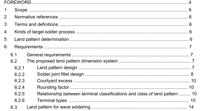
The assumption is that the following dimensions have the necessary and sufficient accuracy: a) component tolerance; c) printed board fabrication tolerance; d) placement tolerance. NOTE Further information on the effect of the above dimensional tolerance on the land pattern can be found in Annex A of IEC 61188-6-1:2021. There are two classes of land pattern relating to the assembly limitations of components and the intended soldering process: • land pattern for wave soldering – For low density product applications, land patterns are designed to accommodate several types of wave soldering applicable to surface mounted components. • land pattern for reflow soldering – The land patterns generated for all device families shall provide a robust solder attachment condition for reflow soldering. 6 Requirements 6.1 General requirements The calculated land pattern geometry for an electronic component can be different depending upon the type of soldering process to be used. Wherever possible, land patterns should be defined in such a manner that are transparent to the attachment process being used. Land pattern designers can use the information contained herein to establish standard configurations not only for manual designs but also for computer-aided design systems. Whether parts are mounted on one side or both sides of the board, subjected to wave soldering, reflow soldering, or other type of soldering, the land pattern and part dimensions should be optimized to insure proper solder joint and inspection criteria. Although patterns are dimensionally defined and since they are a part of the circuit board geometry, they are subject to the reducibility levels and tolerances associated with plating, etching, assembly or other conditioning process.
6.2.3 Courtyard excess Since courtyard excess is influenced by equipment performance, part size accuracy, provision for rework, etc., it should be desirable for the user to decide it. Therefore, in this document, courtyard excess is indicated as a reference value in Annex C. 6.2.4 Rounding factor The rounding factor of the land pattern dimension should be 0,01 mm in general. However, if the rounding factor exceeds 10 % of the dimension, the rounding factor can be decreased to 0,005 mm.
- Previous:IEC 61215-1-2-2021 pdf Terrestrial photovoltaic (PV) modules – Design qualification and type approval – Part 1-2: Special requirements for testing of thin-film Cadmium Telluride (CdTe) based photovoltaic (PV) modules
- Next:IEC 61169-60-2021 pdf Radio-frequency connectors – Part 60: Sectional specification for RF coaxial connectors with push on mating – Characteristic impedance 50 Ohm (type SMPM)
- ISO IEC 27050-4-2021 pdf Information technology — Electronic discovery — Part 4: Technical readiness
- ISO IEC 27036-1-2021 pdf Cybersecurity — Supplier relationships — Part 1: Overview and concepts
- ISO IEC 27013-2021 pdf Information security, cybersecurity and privacy protection — Guidance on the integrated implementation of ISO/IEC 27001 and ISO/IEC 20000-1
- ISO IEC 26580-2021 pdf Software and systems engineering — Methods and tools for the feature- based approach to software and systems product line engineering
- ISO IEC 24735-2021 pdf Information technology — Office equipment — Method for measuring digital copying productivity
- ISO IEC 24711-2021 pdf Information technology — Office equipment — Method for the determination of ink cartridge yield for colour inkjet printers and multi- function devices that contain printer components
- ISO IEC 23544-2021 pdf Information Technology — Data centres — Application Platform Energy Effectiveness (APEE)
- ISO IEC 23510-2021 pdf Information technology — 3D printing and scanning — Framework for an Additive Manufacturing Service Platform (AMSP)
- ISO IEC 23127-1-2021 pdf Information technology — Learning, education, and training — Metadata for facilitators of online learning — Part 1: Framework
- ISO IEC 23126-2021 pdf Information technology for learning, education and training — Ubiquitous learning resource organization and description framework
- BS IEC 62843-2013 pdf Standard for N times 64 kilobit per second optical fiber interfaces between teleprotection and multiplexer equipment
- AS IEC 60601.2.22-2014 pdf Medical electrical equipment Part 2.22: Particular requirements for basic safety and essential performance of surgical, cosmetic, therapeutic and diagnostic laser equipment
- ISO IEC 23127-1-2021 pdf Information technology — Learning, education, and training — Metadata for facilitators of online learning — Part 1: Framework
- IEC 62488-3-2021 pdf Power line communication systems for power utility applications – Part 3: Digital Power Line Carrier (DPLC) Terminals and hybrid ADPLC Terminals
- IEC 61251-2015 pdf Electrical insulating materials and systems – AC voltage endurance evaluation
- BS ISO IEC 15420-2009 pdf Information technology一 Automatic identification and data capture techniques EAN/UPC bar code symbology specification
- BS ISO IEC 19762.5-2008 pdf Information technology一 Automatic identification and data capture (AIDC) techniques – Harmonized vocabulary Part 5: Locating systems
- BS IEC 60860-2014 pdf Radiation protection instrumentation一 Warning equipment for criticality accidents
- ISO IEC 24735-2021 pdf Information technology — Office equipment — Method for measuring digital copying productivity
- ISO IEC 24711-2021 pdf Information technology — Office equipment — Method for the determination of ink cartridge yield for colour inkjet printers and multi- function devices that contain printer components